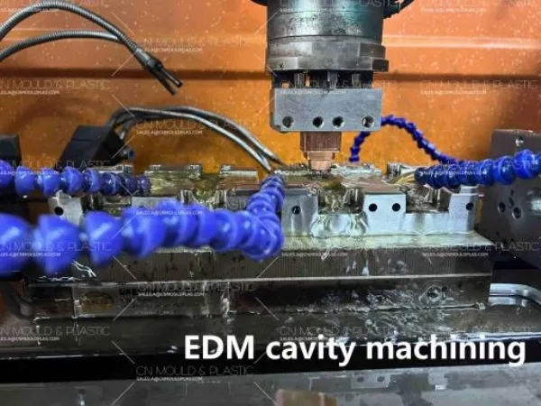
In electrical discharge machining (EDM) of mold cavities, the re‑solidified surface layer — known as the white layer — is an unavoidable byproduct of the process. To maintain surface integrity, the finishing allowance must be sufficient to remove this altered layer, ideally keeping it within 15–20 μm.
However, poor chip evacuation and improper machining conditions can lead to surface defects such as arc burns, carbon buildup, and cracking. Below are six common EDM surface defects, along with their causes and solutions.
Cracks at Edges and Corners
This is typically caused by internal residual stress from low‑temperature tempering or high discharge energy during roughing. To prevent it, use high‑temperature tempered material, reduce discharge energy during roughing, extend discharge off‑time, lower the average machining current, and round the electrode edges and corners to improve heat dissipation.
Cracks at Coarse Carbides
Non‑uniform material structure or segregation is the primary cause. Solutions include inspecting the material structure before machining, increasing average machining voltage, and extending discharge off‑time.
Cracks Found After Polishing
These occur when cracks already exist on the EDM surface or when polishing is insufficient. Address this by using electrode lifting and orbiting techniques, applying small‑current positive‑polarity machining, performing manual polishing, and applying shot peening to the EDM surface.
Corrosion on Rough EDM Surfaces
A rough finish, surface cracks, or residual tensile stress can cause corrosion. Use small‑current positive‑polarity machining and apply glass bead shot peening after EDM to prevent it.
Chrome Plating Peeling on EDM Surfaces
This is primarily caused by surface cracks. Prevent it by using small‑current positive‑polarity machining and applying electrode lifting and orbiting techniques.
Abnormal Arcing and Carbon Build‑up
These are caused by local debris accumulation, insufficient dielectric fluid flushing, short discharge off‑time, or high average machining current. Solutions include ensuring adequate flushing, extending electrode lift stroke and increasing lift speed, and lowering the average machining current.

 English
  français
  Deutsch
  Español
  italiano
  русский
  português
  العربية
  dansk
dansk  Suomi
Suomi  Svenska
  norsk
norsk